Perovskite Solar Hits 30.3% — The First All-Perovskite Tandem to Break the Threshold
NIMTE’s certified result eliminates silicon from the equation entirely. Here’s what the chemistry breakthrough actually did, what the flexible version means for deployment, and what still needs solving before this reaches rooftops.
(Certified)
(Certified)
after 1,000 h
Every solar efficiency record earns a headline. Few change what’s buildable. This one does. In April 2026, researchers at the Ningbo Institute of Materials Technology and Engineering (NIMTE), part of China’s Academy of Sciences, published work in Nature Nanotechnology achieving a certified 30.3% power conversion efficiency in a solar cell made entirely of perovskite — no silicon layer, no silicon substrate. At the same time, their flexible version reached a certified 28.0%, surpassing current commercial silicon module efficiencies. The approach draws from inorganic chemistry — hard-soft acid-base theory applied at the crystal scale — and it addressed both efficiency and stability across two perovskite layers simultaneously. Earlier perovskite durability research solved lifespan problems one layer at a time. This paper did both layers at once.
Certified efficiency milestones across three perovskite device types — a 17-year progression that outpaced silicon’s single-junction development
What an All-Perovskite Tandem Actually Is
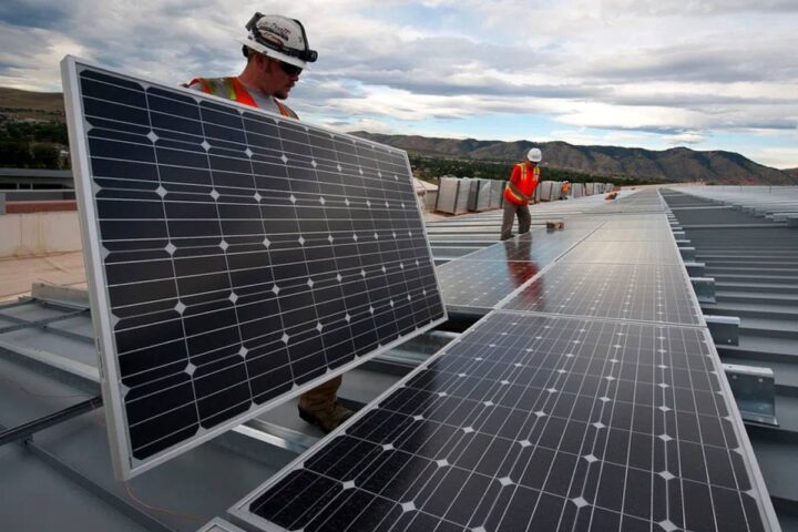
The term “all-perovskite tandem” often gets lost behind headlines about perovskite-silicon tandems — cells that stack a perovskite layer on top of a traditional silicon base. The current silicon-perovskite record is 35.2% (LONGi, NREL-certified, as of the latest Solar Cell Efficiency Tables, Version 67). But silicon carries weight: it is rigid, it constrains form factor, and it ties manufacturing to silicon wafer supply chains. An all-perovskite tandem uses two perovskite layers, each tuned to absorb different parts of the solar spectrum, with no silicon at all. That makes the entire structure thin-film, lightweight, and manufacturable on flexible polymer substrates — surfaces that silicon cannot reach.
| Device Type | Record PCE | Institution | Notes |
|---|---|---|---|
| Si-Perovskite tandem (1 cm²) | 35.2% | LONGi | NREL-certified; efficiency tables v67 |
| All-perovskite rigid tandem | 30.3% | NIMTE / CAS | This paper — first to break threshold |
| All-perovskite flexible tandem | 28.0% | NIMTE / CAS | Certified; no silicon substrate |
| Single-junction perovskite | 26.7% | USTC | NREL-certified (2024) |
| Commercial Si module record | 25.4% | LONGi | HPBC 2.0; Fraunhofer ISE certified (2024) |
| Commercial perovskite-Si module | 24.5% | Oxford PV | Shipped to US utility project, Sept 2024 |
The Chemistry: Why HSAB Theory Made the Difference
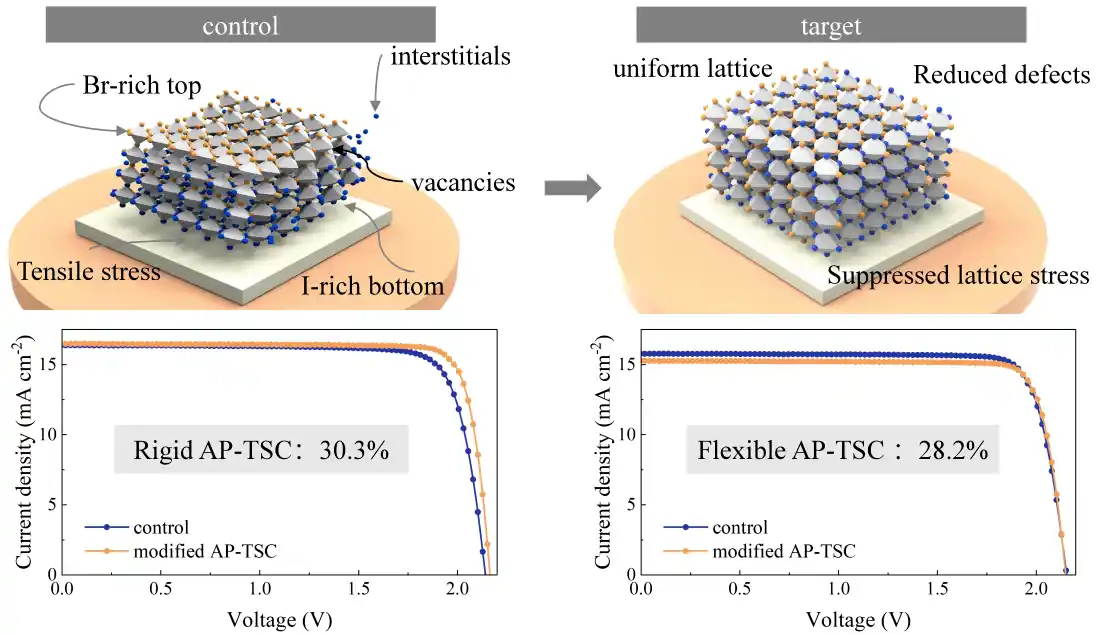
The lead researchers, Prof. Ge Ziyi and Prof. Liu Chang at NIMTE, structured their work around a specific crystallization problem. In all-perovskite tandems, the wide-bandgap top layer (capturing higher-energy blue and UV light) and the narrow-bandgap bottom layer (handling red and near-infrared light) need to grow uniformly without interfering with each other. When they don’t, defects form at grain boundaries, voltages drop, and degradation accelerates — particularly in the narrow-bandgap tin-lead (Sn-Pb) layer, where tin ions oxidise easily and are historically the dominant failure pathway.
Their solution came from Hard-Soft Acid-Base (HSAB) theory — a framework from inorganic chemistry originally introduced by Ralph Pearson in 1963 that predicts which ions selectively bond based on electronic character. The team identified two additives: DFOB⁻ (difluoro(oxalato)borate), a borderline base for the wide-bandgap lead-rich precursor, and BF₄⁻ (tetrafluoroborate), a hard base for the narrow-bandgap tin-lead layer. Each additive coordinates with its own precursor system, synchronising nucleation and crystal growth without cross-interference. The result: uniform films across both layers, reduced halide redistribution, and fewer structural defects at grain boundaries.
“The findings provide a pathway to simultaneously improve efficiency and durability in both rigid and flexible devices, thereby advancing the development of lightweight, scalable photovoltaic technologies.”
— Prof. Ge Ziyi & Prof. Liu Chang, NIMTE / Chinese Academy of SciencesThe efficiency improvement was measurable at each level. The wide-bandgap sub-cell rose from 18.5% to 20.1%. The narrow-bandgap sub-cell improved from 21.6% to 23.3%. Combined in a two-terminal monolithic configuration, the rigid tandem achieved 30.3% certified — the first all-perovskite tandem to break that threshold with independent certification. Fill factor reached 85.2%, and open-circuit voltage hit 2.16 V, both reflecting reduced energy loss across the stacked device.
The Flexible Version at 28.0%: Why It Matters
The flexible version at 28.0% deserves equal weight in this story. For context: Oxford PV’s commercially shipped perovskite-silicon modules achieve 24.5% module efficiency, and LONGi’s crystalline-silicon module record stands at 25.4%. The 28.0% flexible all-perovskite cell surpasses both — without any silicon and without a rigid substrate. A bendable all-perovskite solar surface is viable for applications that rigid silicon cannot serve: vehicle rooftops and body panels, curved building facades, portable charging surfaces, and lightweight off-grid modules. Panasonic’s perovskite glass work pointed toward building-integrated photovoltaics in dense urban settings; flexible all-perovskite tandems take that further by removing the glass substrate from the equation entirely for certain applications.
Stability: What 92% After 1,000 Hours Actually Means
The 92% retention after 1,000 hours of maximum power point tracking needs honest context. Commercial silicon solar panels carry 25-year performance warranties — roughly 219,000 hours of outdoor operation. The 1,000-hour test is an industry-standard early checkpoint, not a lifespan projection. It is a strong baseline result. NREL’s salt-layer single-junction work retained 98% at 2,100 hours at 65°C, providing a useful comparison point. But the gap between 1,000-hour indoor data and 25-year outdoor durability remains the central challenge for all perovskite solar technologies. IEC 61215 accelerated aging protocols — damp-heat, UV irradiation, thermal cycling — are the next validation hurdles this device must clear.
1,000-hour lab tests are a necessary first gate — not a commercial lifespan claim. The field’s move from lab cells to 25-year outdoor modules requires IEC 61215 damp-heat, UV cycling, and thermal shock protocols across large-area substrates. Alumina nanoparticle durability research and parallel NREL salt-layer work are building the evidence base for these protocols. Until module-scale multi-year outdoor data exists, efficiency records and stability milestones should be read as directional, not deployable.
Lead Content, Circularity, and Responsible Design
One point largely absent from other coverage: lead content and circular product design. Both perovskite layers in this device contain lead. As perovskite solar approaches commercialisation, the EU’s Ecodesign for Sustainable Products Regulation (ESPR) — which entered into force in July 2024 — is progressively rolling out requirements through product-specific delegated acts under its 2025–2030 working plan. Digital Product Passports (DPPs) will be required product by product as each delegated act is finalised, not as a blanket 2026 requirement across all energy products. That means lead content declarations, recycling instructions, and material recovery pathways need to be built into perovskite product design now — in anticipation of those requirements, not after. The research community’s focus on efficiency and stability needs a parallel track in responsible materials design.
The push to triple clean energy by 2030 is only durable if the products delivering it can be safely recovered at end of life.
Cost and the Path to Deployment
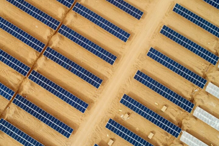
On cost: Independent analyses published in 2025 estimate all-perovskite module manufacturing at approximately $0.57 per watt at current lab-to-pilot scale, with projections of $0.29–0.42/W at commercial scale. Materials account for roughly 70% of manufacturing cost, and perovskite precursors are solution-processable at low temperatures — meaning existing coating and printing infrastructure can be adapted rather than rebuilt. Global solar capacity is on track toward 700 GW annually by 2030, and cost-competitive flexible formats could accelerate deployment in markets where rigid-panel logistics constrain installation — including large parts of the Global South, where lightweight distributed energy access is an acute need.
Five Questions This Research Actually Answers
Where Things Stand
The work from NIMTE, published in Nature Nanotechnology in April 2026, established a certified 30.3% power conversion efficiency in a rigid all-perovskite tandem solar cell and 28.0% in a flexible configuration. The wide-bandgap sub-cell improved from 18.5% to 20.1%; the narrow-bandgap sub-cell from 21.6% to 23.3%. The device retained 92% of its initial efficiency after 1,000 hours of maximum power point tracking, with an open-circuit voltage of 2.16 V and a fill factor of 85.2%.
The chemical hardness-guided additive approach — DFOB⁻ for the wide-bandgap layer, BF₄⁻ for the narrow-bandgap layer — addressed crystallisation synchronisation between two chemically distinct perovskite systems in a single fabrication step. The research was led by Prof. Ge Ziyi and Prof. Liu Chang at the Ningbo Institute of Materials Technology and Engineering, Chinese Academy of Sciences.
The certified 30.3% threshold, the flexible variant’s efficiency above commercial silicon modules, the material-level approach to tin-layer stabilisation, and the remaining gaps — scale, long-term durability, and circular product design — were the central points covered here. For further context on where perovskite solar has come from, see earlier durability research and NREL’s salt-layer efficiency work.